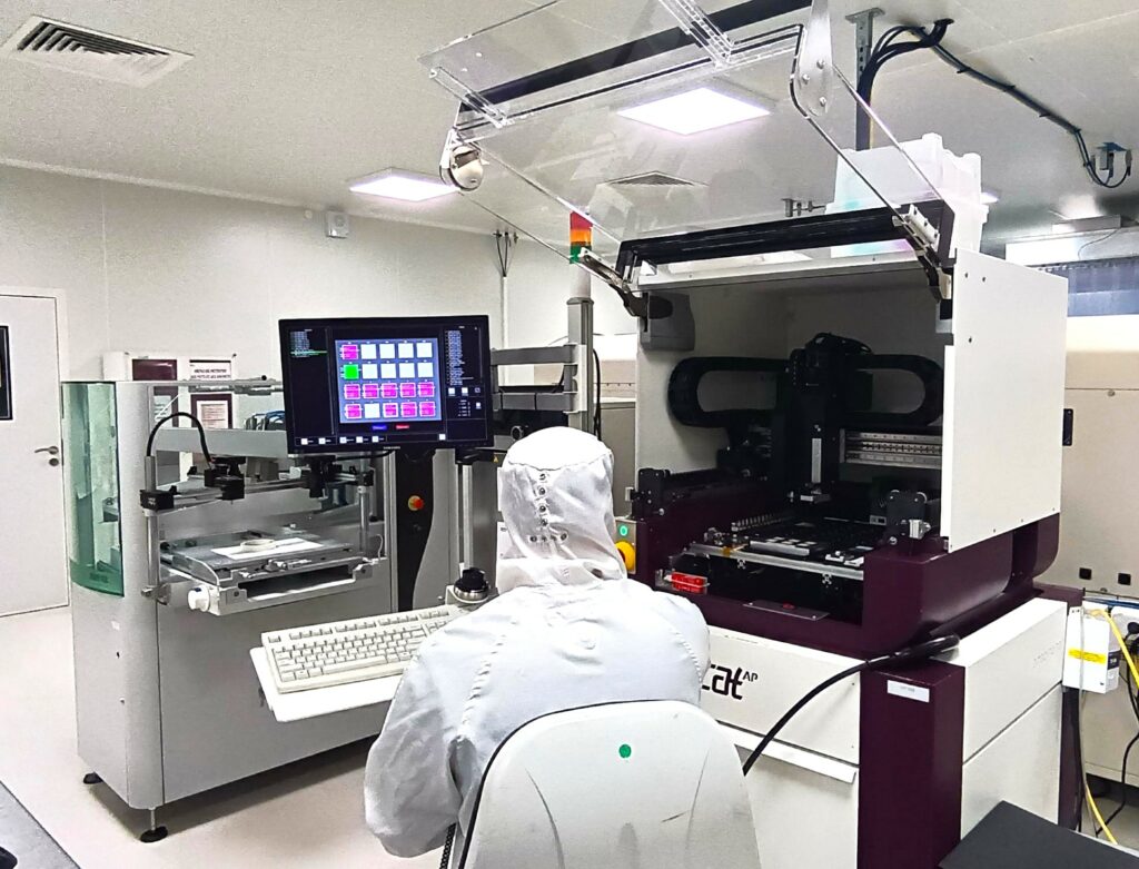
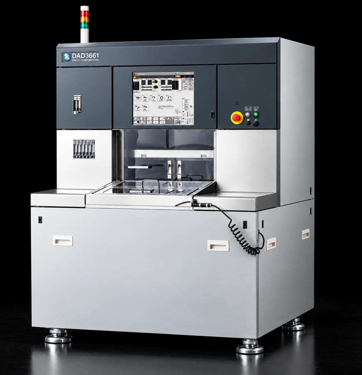
SERMA Microelectronics is strengthening its industrial capabilities with the integration of a new wafer dicing system: the DISCO DAD3661. This new equipment now enables the processing of wafers up to 12 inches, with operations carried out in-house in France, from sawing through to assembly.
A new wafer sawing capability for 12-inch wafers
SERMA Microelectronics continues to expand its manufacturing capabilities with the integration of a new DISCO DAD3661, dedicated to wafer sawing and dicing for wafers up to 12 inches.
This new equipment complements SERMA Microelectronics’ existing capabilities and enables us to offer customers comprehensive wafer processing, from dicing through to assembly, directly in France.
The objective is to support projects requiring greater flexibility, precision and process control, particularly for high-value-added microelectronics applications.
A solution designed for complex wafers and layouts
The new DAD3661 offers a wide range of processing capabilities:
- Wafer handling up to 12 inches
- Compatible with UV Tape and Blue Tape
- Dual-spindle technology enabling advanced step cutting
- Non-sacrificial MPW – Multi Project Wafer – processing
- Die extraction suitable for complex reticle layouts
SERMA Microelectronics can therefore handle a wide variety of wafer configurations and address specific dicing requirements depending on component technologies and architectures.
Silicon, GaAs, Sapphire, GaN, Glass…
This new capability supports a broad range of materials used throughout the semiconductor industry: Silicon, GaAs, Sapphire, GaN, Glass…
This versatility enables SERMA Microelectronics to address the requirements of multiple markets and applications, including space, aerospace, telecommunications, industrial and advanced technology sectors.
A complete ecosystem dedicated to 12-inch wafer processing
The integration of the DAD3661 is supported by additional dedicated equipment, enabling SERMA Microelectronics to control the entire wafer processing workflow.
Our capabilities include:
- Frame Film Mounter
For wafer preparation and mounting onto film prior to the dicing process. - LED UV Film Release System
For controlled UV film treatment and easier handling during post-dicing operations. - Automatic Cleaning System
For wafer cleaning and preparation before subsequent process steps.
Together, these systems provide SERMA Microelectronics with a complete processing ecosystem dedicated to 12-inch wafers.
Frame Film Mounter
LED UV Film Release System
Automatic Cleaning System
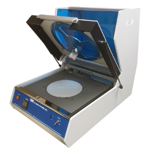
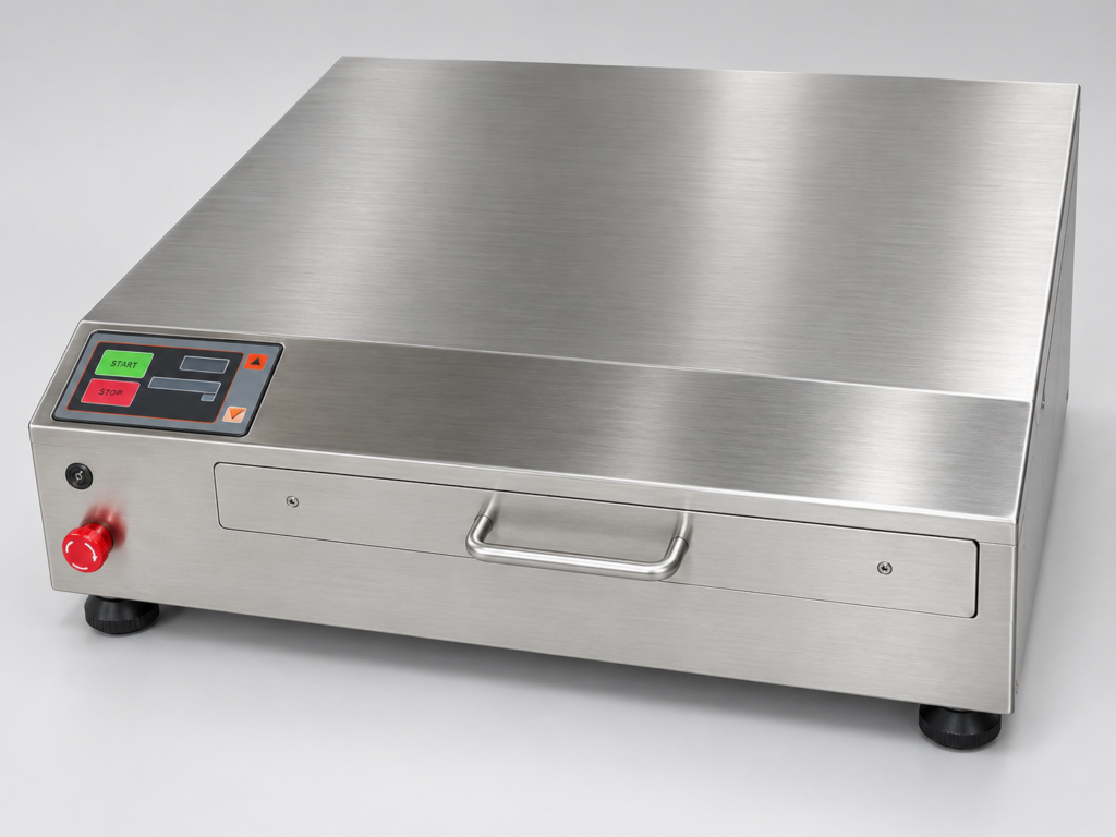
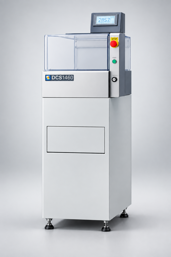
Automated expansion for easier pick & place
An automated expansion solution can also be incorporated into the process after dicing.
Expansion increases the spacing between dies, making them easier and safer to handle during downstream operations.
It helps to:
- Increase spacing between dies
- Facilitate pick & place operations
- Reduce the risk of chip-out during die handling
- Improve handling security for both automated and manual processes
An in-house process managed in France
With this new capability, SERMA Microelectronics further strengthens its offering in wafer-level processing and microelectronics assembly.
From wafer preparation and dicing to die handling and assembly, the different process steps can be carried out in-house at our facilities in France.
This control over the processing chain provides customers with greater flexibility, responsiveness and process control throughout their projects.
Do you have a 12-inch wafer sawing or wafer processing project?
Contact the SERMA Microelectronics team to discuss your requirements and define the most suitable process for your application.