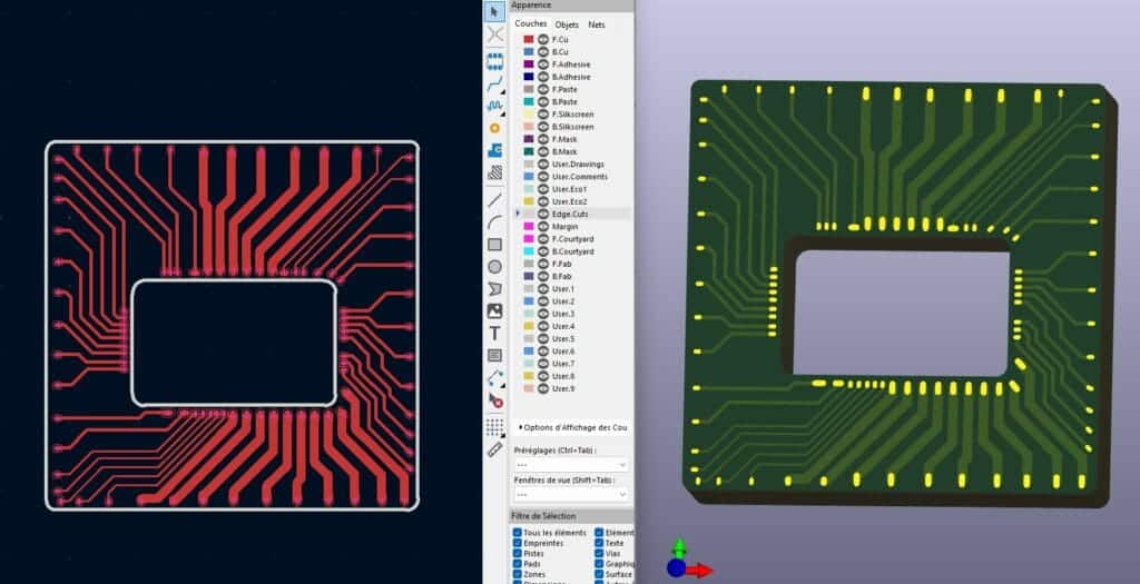
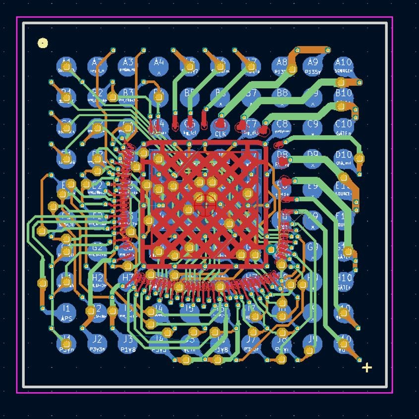
MENU
ENGINEERING

Electronic design

Based on your input data (block diagram, parts list, mechanical constraints), we offer to produce the design dossier for the substrate(s) related to your product: modules, hybrids, macro-components, for example.

The term “substrate” refers to any type of technology adapted to chip and component placement, such as:

  • Thick-film substrate
  • Thin-film substrate
  • Co-fired (LTCC, HTCC)
  • Organic support structure (Epoxy, Flex, polyamide, SMI)
  • DBC
  • ALN

These services related to the production of the design dossier are performed using CAD tools: CADENCE for mainly digital PCBs and substrates, or ZUKEN. Depending on the needs, they may incorporate thermal and/or electrical simulation.

These developments take into account DFM/DFT imperatives and special care is taken regarding testability aspects (e.g. for large-scale production and products requiring a high level of reliability).

The post-placement and post-routing reviews, as well as the pre-production launch review, are led by SERMA Microelectronics depending on the complexity and criticality of the project.

LAYER TOP (PCB)

LAYER TOP
(substrat sérigraphié)

LAYER CONDUCTOR-2
(substrat sérigraphié)