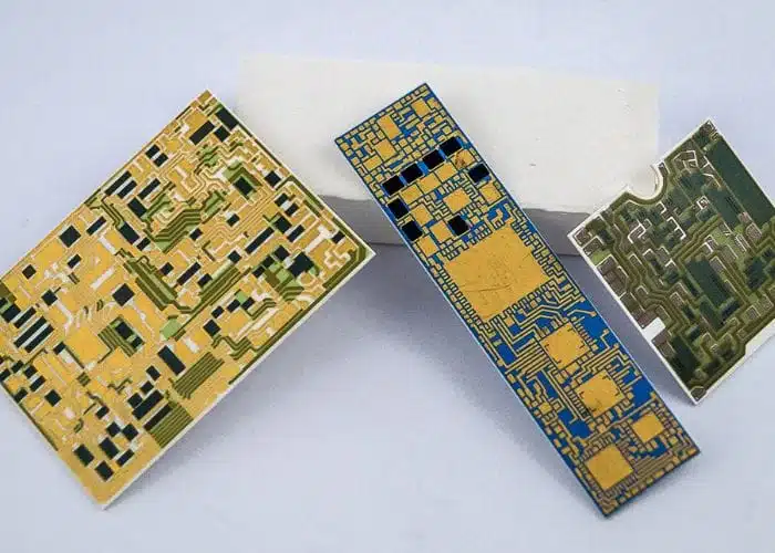
“Thick-film technology”, as it is known, enables us to produce substrates with a very high degree of reliability:
- Minimalist support structure
- Inalterable deposit
- Resistance to very high temperatures
- Precision adjustment of resistors
- Support structure perfectly suited to chip placement techniques (bonding and/or brazing) and bonding (thermosonic technology on non-elastic substrate).
This technology is therefore widely used in all the potential solutions available for placing and interconnecting electronic components.
We have been serving this market since the 1980s, positioned in the manufacture of hi-tech small and medium batch productions (multi-layers, adjusted resistance, space substrates, etc.).
SERMA Microelectronics has an end-to-end production line for this type of substrate :
- Cutting devices for ceramic plates (CO2 laser)
- Laboratory for producing films and screens
- Stencil-printing machines specifically adapted to thick-film technology
- Drying oven
- Firing oven
- Dynamic adjustment of resistors by LASER ablation
- Electrical test means, capacitive tests and flash tests
