As the miniaturization of electronic components becomes increasingly crucial, flip-chip technology has emerged as an essential solution for integrated circuit interconnection and is being adopted by more and more semiconductor manufacturers.
However, access to this technology remains complex, if not impossible, for many industrial players who cannot acquire entire wafer lots and instead rely on Multi-Project Wafers (MPW) which allows multiple designs or projects to share tooling and fabrication costs for microelectronic wafers.
Once the individual chips are recovered, their full potential remains limited and their characteristics cannot be exploited to their maximum. Given their metallization pads, the only available solution is wire bonding, which unfortunately introduces parasitic effects that degrade signal propagation and overall component performance.
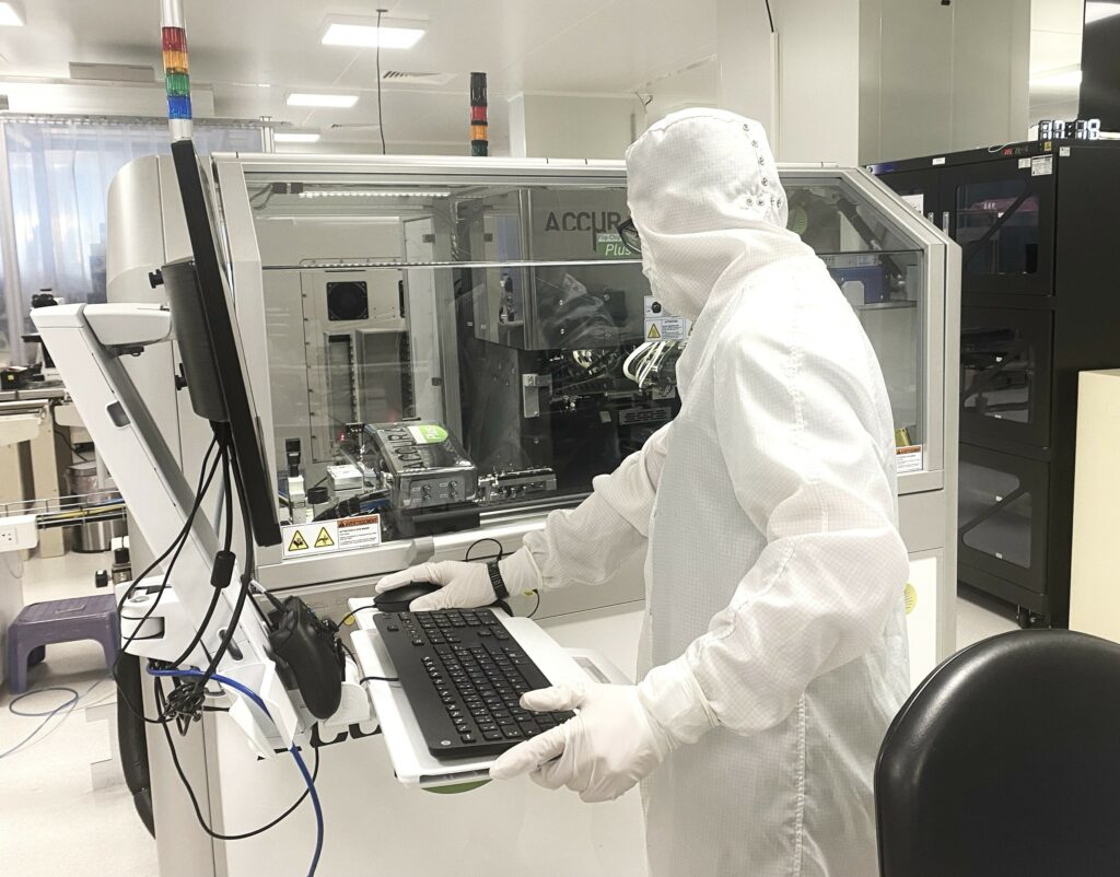
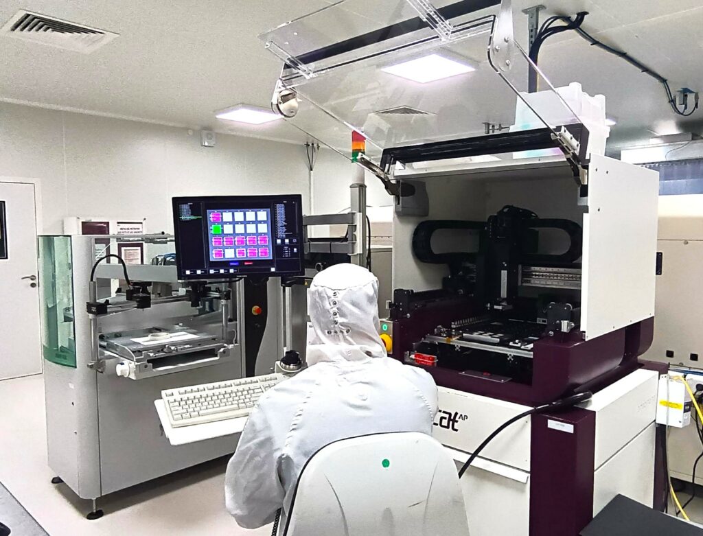
SERMA Microelectronics developed an exclusive service for UBM creation and re-metallization, available at both the chip and wafer level!
Our goal? To transform wire-bonded components into flip-chip components, ready for PCB soldering, ensuring seamless integration and optimized performance.
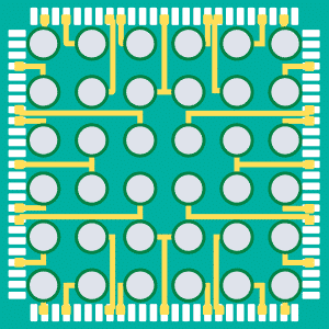
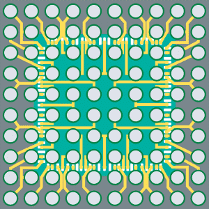
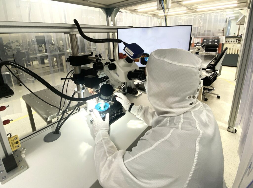
But we go even further! We offer external layer redistribution (Fan-In and Fan-Out) to adapt electrical connections to your configuration.
With Fan-In and Fan-Out approaches, you can:
✅ Achieve a high level of miniaturization
✅ Reduce parasitic effects
✅ Enhance electrical and thermal performance
With more than 30 years of expertise at your Service, SERMA Microelectronics delivers cutting-edge packaging solutions tailored to your prototyping and production needs!